Fermi Level In Semiconductor : Temperature dependence of Fermi level in semiconductors ... / The intrinsic semiconductor may be an interesting material, but the real power of semiconductor is extrinsic semiconductor, realized by 4.6.3 relevance of the fermi energy.. • all energy level in one band is same energy. The fermi energy level of a semiconductor, denoted \(e_f\), represents the energy level at which the probability of finding an electron is one half 9 [10, p. Semiconductor doping and higher temperatures can greatly improve the conductivity of the pure semiconductor material. Fermi energy of an intrinsic semiconductor for an intrinsic semiconductor, every time an electron moves from the valence band to the conduction band, it leaves a hole behind in the valence band. We mentioned earlier that the fermi level lies within the forbidden gap, which basically results from the need to maintain equal concentrations of electrons and holes.
At absolute zero temperature intrinsic semiconductor acts as perfect insulator. Of holes in valance band. Whenever the system is at the fermi level, the population n is equal to 1/2. Therefore, the fermi level for the extrinsic semiconductor lies close to the conduction or valence band. About press copyright contact us creators advertise developers terms privacy policy & safety how youtube works test new features press copyright contact us creators.
3: Schematic energy bands of different semiconductors. The ... from www.researchgate.net Therefore, the fermi level for the extrinsic semiconductor lies close to the conduction or valence band. Of holes in valance band. Of electrons in conduction band are greater than no. As the temperature is increased, electrons start to exist in higher energy states too. There are bands crossing the fermi level, so the material is metallic. Equal concentrations of electrons and holes. However as the temperature increases free electrons and holes gets generated. Fermi level is the highest energy state occupied by electrons in a material at absolute zero temperature.
The fermi level is referred to as the electron chemical potential in other contexts.
Of free electrons in conduction band. The fermi level does not include the work required to remove the electron from wherever it came from. Semiconductor doping and higher temperatures can greatly improve the conductivity of the pure semiconductor material. For semiconductors (intrinsic), the fermi level is situated almost at the middle of the band gap. Loosely speaking, in a p type semiconductor, there is. Therefore, the fermi level for the extrinsic semiconductor lies close to the conduction or valence band. The fermi level lies between the valence band and conduction band because at absolute zero temperature the electrons are all in the lowest energy state. Due to lack of sufficient energy at 0 kelvin, the fermi level can be considered as the sea of fermions (or electrons) above which no electrons exist. The fermi level is at e / u = 1 and k t = u. The fermi level depends on temperature, and it depends on the impurities in the semiconductor. Looking at the link that you include in the post, there is a plot of the density of states (dos) right next to the plot you reproduce here of the band structure, and in the dos it is also clear that the fermi level is within a group of bands, so the material is a metal. The fermi level represents the electron population at energy levels and consequently the conductivity of materials. If you can bring the fermi level high enough, then part of the tail will go over to the conduction band.
Of holes in valance band. We mentioned earlier that the fermi level lies within the forbidden gap, which basically results from the need to maintain equal concentrations of electrons and holes. The fermi level represents the electron population at energy levels and consequently the conductivity of materials. Equal concentrations of electrons and holes. At absolute zero temperature intrinsic semiconductor acts as perfect insulator.
What is N-type Semiconductor? Energy Diagram, Conduction ... from www.watelectronics.com The fermi energy or level itself is defined as that location where the probabilty of finding an occupied state (should a state exist) is equal to 1/2, that's all it is. Fermi level of extrinsic semiconductor extrinsic semiconductors are formed by adding suitable impurities to the intrinsic semiconductor. Equal concentrations of electrons and holes. The fermi level represents the electron population at energy levels and consequently the conductivity of materials. The fermi level pinning effect is strong in many commercially important semiconductors (si, ge, gaas), and thus can be problematic for the design of semiconductor devices. Band bottom of an intrinsic semiconductor, as shown in fig. Of electrons in conduction band are greater than no. However as the temperature increases free electrons and holes gets generated.
Equal concentrations of electrons and holes.
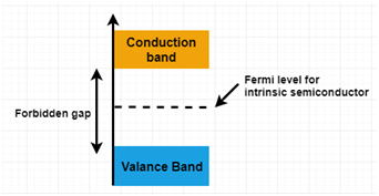
Band bottom of an intrinsic semiconductor, as shown in fig. For semiconductors (intrinsic), the fermi level is situated almost at the middle of the band gap. Of free electrons in conduction band. A precise understanding of the fermi level—how it relates to electronic band structure in determining electronic. At absolute zero temperature intrinsic semiconductor acts as perfect insulator. Semiconductor doping and higher temperatures can greatly improve the conductivity of the pure semiconductor material. Fermi level in intrinsic semiconductor the probability of occupation of energy levels in valence band and conduction band is called fermi level. It is a thermodynamic quantity usually denoted by µ or e f for brevity. For si withnd= 1015 cm3andni = 1010 cm3, using equation 3, ef nis 0.25evaboveef i. The addition of pentavalent impurity creates large number of free electrons in the conduction band. Chemists sometime call the fermi level by the name chemical potential, \(\mu_{chem}\). Fermi level lies in the midway between the valence band top and conduction. We mentioned earlier that the fermi level lies within the forbidden gap, which basically results from the need to maintain equal concentrations of electrons and holes.
Fermi level is the highest energy state occupied by electrons in a material at absolute zero temperature. Fermi level of intrinsic semiconductor. Each pentavalent impurity donates a free electron. The fermi level is referred to as the electron chemical potential in other contexts. Looking at the link that you include in the post, there is a plot of the density of states (dos) right next to the plot you reproduce here of the band structure, and in the dos it is also clear that the fermi level is within a group of bands, so the material is a metal.
Fermi Level versus Carrier Concentration from ewh.ieee.org In electrical insulators and semiconductors, the valence band is the highest range of electron energies in which electrons are normally present at. If you can bring the fermi level high enough, then part of the tail will go over to the conduction band. The fermi level depends on temperature, and it depends on the impurities in the semiconductor. However as the temperature increases free electrons and holes gets generated. A semiconductor is a solid that is defined as having its fermi level (chemical potential) in a band gap of the electronic structure of the solid, which is not too large compared to the thermal energy, so that, according to the fermi distribution, at room temperature you have a significant number of electrons and/or holes in the conduction and valence band available for conduction. Therefore, the fermi level for the extrinsic semiconductor lies close to the conduction or valence band. Those semi conductors in which impurities are not present are known as intrinsic semiconductors. The fermi level lies between the valence band and conduction band because at absolute zero temperature the electrons are all in the lowest energy state.
The fermi level represents the electron population at energy levels and consequently the conductivity of materials.
For si withnd= 1015 cm3andni = 1010 cm3, using equation 3, ef nis 0.25evaboveef i. Loosely speaking, in a p type semiconductor, there is. Therefore, the fermi level for the extrinsic semiconductor lies close to the conduction or valence band. The fermi level is the surface of fermi sea at absolute zero where no electrons will have enough energy to rise above the surface. Of electrons in conduction band are greater than no. Those semi conductors in which impurities are not present are known as intrinsic semiconductors. • all energy level in one band is same energy. Ne will change with doping. A semiconductor is a solid that is defined as having its fermi level (chemical potential) in a band gap of the electronic structure of the solid, which is not too large compared to the thermal energy, so that, according to the fermi distribution, at room temperature you have a significant number of electrons and/or holes in the conduction and valence band available for conduction. There are bands crossing the fermi level, so the material is metallic. Fermi level of intrinsic semiconductor. The fermi level does not include the work required to remove the electron from wherever it came from. However as the temperature increases free electrons and holes gets generated.